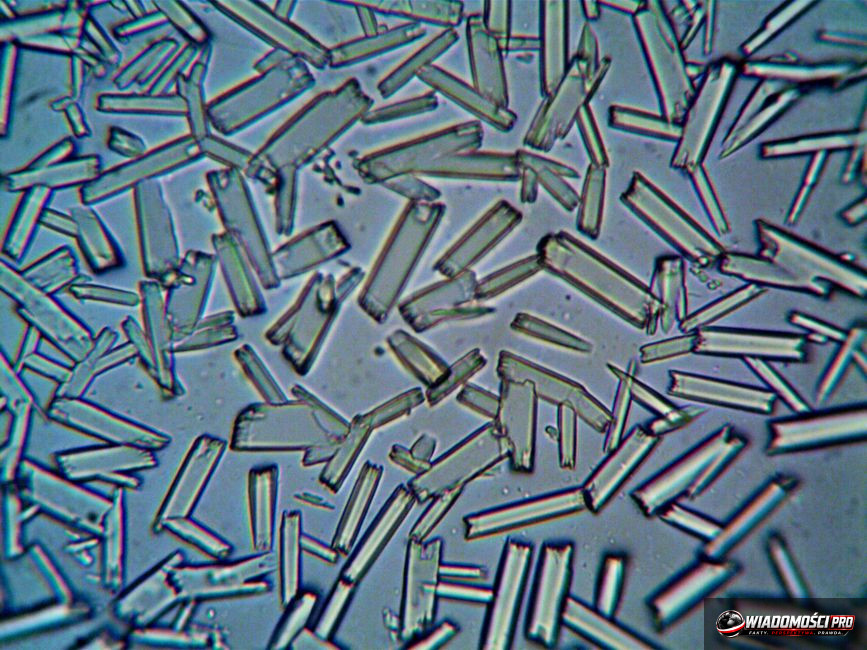
New direct conversion technology eliminates the need for expensive sensors; however, as of September 19, 2026, there are no confirmed market prices or names of specific products available to consumers. This technology will allow for cheap thermal imagers, but not before 2028. This solution is based on the use of thin-film perovskite structures that convert infrared photons directly into visible light, bypassing the costly stage of digital electrical signal processing. Although the vision of a thermal imager in every smartphone fires the imagination, implementing this method into mass production remains a challenge that modern consumer electronics assembly lines have not yet faced.
The physics of the breakthrough: How infrared becomes a visible image
Modern thermal imaging is a process requiring multi-stage signal processing, which burdens the budget of every device manufacturer. Traditional microbolometer sensors, based on vanadium oxide or amorphous silicon, act as thermal energy detectors. This energy must be converted into electrical impulses. The signal goes to an ROIC (Readout Integrated Circuit). There, it is amplified, filtered, and only after digital conversion and intensive processing by an image processor does it reach the display. This is a chain that is inherently prone to noise, requires complex cooling, and generates high energy costs.
The new concept, described in scientific publications by, among others, research teams from MIT and materials engineering centers, shifts the center of gravity to the converting layer. Instead of building an array that only counts photons, engineers are focusing on thin-film materials based on perovskites. These materials exhibit unique photon upconversion capabilities. When infrared radiation, typically in the long-wave LWIR range, hits a surface coated with perovskite, there is an immediate re-emission of energy in the form of visible light. The thermal image thus becomes an optical image. It can be recorded using a standard CMOS sensor, known from cameras.
From the point of view of solid-state physics, this approach eliminates the most critical point of production: the need to manufacture sensors with a high temperature sensitivity coefficient, which must be enclosed in sealed, vacuum housings. In direct conversion, the perovskite array acts as a passive wavelength converter. If this method is refined, a thermal imaging camera will become technically similar to an ordinary digital camera. There is no need for advanced image processors to extract the signal from the microbolometer noise. The entire operation is taken over by the crystal structure of the material.
Why was thermal imaging a luxury until now?
The barrier to entry into the world of thermal imaging did not result from a lack of desire by manufacturers, but from the physical limitations of infrared optics. Standard silicon glass, used to make lenses in smartphones, is opaque to infrared radiation above 1.5 micrometers. To record heat emitted by objects at room temperature, i.e., in the 8–14 micrometer band, it is necessary to use germanium lenses. This element is a rare raw material, difficult to process, and extremely expensive.
The production costs of thermal imaging cameras were determined by three main factors, which in recent years have been an insurmountable barrier for the mass market. First, the microbolometer sensor must be placed in a vacuum to minimize thermal conductivity between pixels. Such a design necessitates the use of expensive metal-ceramic housings. Second, the aforementioned germanium optics require precise grinding, which raises the price of a single lens to the level of several thousand zlotys. Third, software for non-uniformity correction and advanced noise reduction algorithms required expensive licenses and dedicated computing hardware.
The current cost breakdown for producing a professional thermal imaging module is as follows:
- Microbolometer sensor: 1500–5000 PLN depending on resolution.
- Germanium lens: 800–2500 PLN per single piece.
- Vacuum housing and control electronics: 1200–3000 PLN.
The new direct conversion technology has a chance to radically cut costs because it allows for the use of cheaper substrates and the abandonment of vacuum. If the perovskite layer can be applied directly to a CMOS sensor, we will eliminate the need for a separate, expensive infrared sensor. Instead of building a dedicated camera, we will be able to add thermal imaging functionality to existing image sensor production infrastructure. This is a technological leap that the industry has not seen in decades.
Market potential: Smartphone as a diagnostic tool
The ability to integrate an infrared converter with a smartphone sensor opens the door to applications that have so far been the domain of specialized technical teams. In the construction industry, a key problem is the detection of thermal bridges. Currently, a contractor wanting to check the tightness of attic insulation must hire an auditor with a professional camera or invest in equipment that takes years to pay for itself. If direct conversion technology reaches mobile devices, diagnostics will become a common work standard.
Equally important is safety and electrical diagnostics. Imagine an electrician who, using a phone, verifies overheating contacts in a switchgear instead of taking point measurements with a multimeter. Such an approach allows for the detection of failures at the stage of early thermal symptoms, which drastically increases the safety of installation operation. In the security sector, a night observation function built into a standard smartphone would change the way we approach home surveillance, eliminating the need to install complex night vision systems.
However, behind this optimism lies a hard technological reality. Adapting CMOS sensors to work with perovskites requires solving problems with so-called signal crosstalk between visible and infrared photons. The software must be able to distinguish light falling directly on the sensor from light coming from the converter. This is a task for imaging algorithm engineers, who must create new processing software stacks before the first device reaches the hands of consumers.
Engineering challenges and uncertainty of results
Moving from the laboratory phase to mass production is a process that usually takes about two years in consumer electronics. Currently, engineers are focusing on the chemical stability of the converting layers. Perovskites, despite their high efficiency, are materials sensitive to moisture and UV radiation. Long-term exposure to atmospheric conditions can lead to degradation of the crystal structure. In practice, this would mean a loss of image quality after a few months of use.
Another challenge is conversion linearity. For a thermal image to be useful, we must be sure that the converting material maintains constant characteristics over a wide range of ambient temperatures. If conversion efficiency drops drastically as the device temperature increases, we will be dealing with a tool that requires frequent calibration. What works in a laboratory under controlled conditions may prove unreliable in the field.
The silence of leading sensor manufacturers, such as Sony or Samsung, is telling. The lack of official announcements about cooperation with perovskite laboratories suggests that we are not yet at the stage of ready-to-implement projects. Investors who expect immediate market changes must understand that the consumer electronics industry is conservative about introducing new types of semiconductor materials. Every change in raw materials involves the need to rebuild entire production lines, which costs billions of dollars.
Impact on the construction industry and safety
The democratization of diagnostic tools is not just a matter of price, but above all a change in technical culture. In construction, we often encounter a situation where the contractor simply does not have the tools to verify their work. A thermal imaging camera in a smartphone could become a digital level, a tool that every professional carries in their pocket. This would allow for the elimination of assembly errors on an ongoing basis, during the work, and not after the building is handed over for use.
In the security sector, cheap thermal imaging is an opportunity to increase the range of perimeter protection systems. Currently, infrared barriers are either point-based or require expensive installation of high-resolution thermal imaging cameras. If direct conversion modules are cheap enough, they can become part of standard video surveillance systems, enriching the image with a thermal layer without the need to install additional, expensive sensors.
We must remember the limits of precision. Professional thermal imaging cameras used in the chemical or aviation industries must meet strict measurement accuracy standards. Consumer devices, even those based on new technology, will have a margin of error significantly higher than certified industrial-grade devices. Professionals will likely continue to use expensive, certified units, while the new technology will dominate the market for everyday use.
Prospects for 2027 and beyond
Looking at the calendar, 2027 is often cited in analyses as a watershed moment for the commercialization of perovskite technologies. If we see the first announcements of cooperation with large sensor factories in the coming quarters, we will be able to talk about a real implementation schedule. Without such announcements, the project remains only on the roadmap of physical laboratories.
Healthy skepticism toward loud announcements is necessary. The history of electronics knows hundreds of projects that performed well in laboratory tests but did not survive the process of scaling production to millions of units. The problem of material purity, repeatability of chemical processes, and heat management inside a smartphone housing are challenges that verify the reality of every technological promise.
Consumers should be prepared for the fact that even if the technology hits the market in 2028, the initial devices will be expensive and full of software flaws. The first generation of smartphones with thermal imaging will likely serve as a testing ground for early adopters, not as a ready, reliable work tool. Time will tell if the physics of direct conversion proves resilient enough to harsh market conditions.
What this means for you
As a consumer, you gain hope for a tool that has so far been reserved for professionals with a high budget. The catch lies in the scale of production and the durability of the materials. If manufacturers manage to solve the problems with perovskite degradation, thermal imaging will become as common as macro or wide-angle modes in phones are today. If, however, the engineering challenges prove too costly, this technology will remain in a niche, and we will have to wait a long time for a real change in thermal imaging.
Questions and answers
Will this technology replace traditional thermal imaging cameras?
It may replace budget devices for amateur and semi-professional applications. Specialized industrial units, requiring high metrological precision and certification, will continue to rely on advanced microbolometer sensors, as their operating characteristics are more predictable in extreme conditions.
When will it be possible to buy a smartphone with such a function?
Currently, there is no schedule for introducing the technology into mass production. Any dates appearing in the media are speculation, as no cooperation with any of the major mobile electronics manufacturers has been confirmed.
Does image conversion affect photo quality?
This technology requires applying a converting layer to the sensor. There is a risk that this will affect the quality of the visible image, especially in terms of color reproduction and sharpness, which is why engineers are working on circuits that allow this layer to be turned off or bypassed during daily use of the camera.
Material analysis: Why perovskites?
The choice of perovskites as a material for infrared conversion is not accidental. These chemical compounds with an ABX3-type crystal structure possess unique optoelectronic properties. Their greatest advantage is the ability to easily "tune" the bandgap by changing the chemical composition. This means that engineers can precisely control which infrared wavelengths will be absorbed and processed into visible light. Unlike traditional semiconductors, where crystal growth processes are extremely energy-intensive and require high temperatures, perovskites can be applied using solution methods, including spraying or the "spin-coating" technique. This paves the way for low-cost production methods.
Despite these advantages, the market must face the fact that perovskites are ionic materials. Their structure, although efficient in conversion, shows a tendency for ion migration in the presence of an electric field. In practice, this means that after some time of device operation, a so-called "drift" of electrical parameters may occur, which manifests as a loss of image quality or an increase in noise levels. Scientists are currently working on encapsulation techniques, i.e., tightly sealing perovskite layers in polymers or metal oxides to isolate them from external factors. Without this protection, any device with such an array would be susceptible to degradation in high humidity conditions.
Production logistics and supply chain
Implementing direct conversion technology requires not only laboratory successes but also a change in the entire supply chain in the semiconductor industry. Currently, CMOS sensors are produced in highly automated lithographic processes, where the cleanliness of the environment is counted in units of particles per cubic meter of air. Introducing perovskites into this process means the need to create "hybrid" production lines. It is necessary to combine traditional silicon lithography with chemical deposition of active layers.
Large manufacturers, such as TSMC or Samsung, are known for not taking risks until the process reaches an efficiency of 99.9% yield of functional chips from a single silicon wafer. In the case of perovskites, achieving such high repeatability over large areas (typical for smartphone sensors) is currently out of reach. Any minor non-uniformity in the perovskite layer on the surface of the CMOS sensor will result in "dead pixels" or areas with different thermal sensitivity. This is a challenge that engineers must solve before any product hits store shelves.
Perspective for professionals
For professionals who use thermal imaging cameras daily in construction or electrical diagnostics, the new technology may seem like a threat to their professional equipment. It is worth noting, however, that professional units, such as those offered by companies like FLIR or Testo, offer much more than just a thermal image. These are advanced tools for radiometric measurement that allow for the precise determination of the temperature of every point on the image with an accuracy of a fraction of a degree Celsius.
Direct conversion technology in smartphones, even if it reaches the commercial phase, will serve as a visual indicator, not a precise measuring tool. It will be a difference similar to that between a professional camera with a full-frame sensor and a smartphone. Both devices take pictures, but their use in professional photography is quite different. The new technology will most likely fill the gap between the lack of any thermal preview capability and professional diagnostic equipment. This is a market expansion that will allow for faster initial assessment of the situation, but will not eliminate the need for certified equipment in critical situations.
Are we in for a repeat of history?
The history of consumer electronics is full of technologies that were supposed to be groundbreaking and ultimately remained in the shadows. Suffice it to mention early attempts to integrate air quality sensors into smartphones, which were supposed to become a standard and ultimately disappeared from most models due to their short lifespan and low accuracy. Will perovskite thermal imaging share this fate?
The answer depends on whether engineers can answer the question of longevity. Consumers expect a smartphone to work flawlessly for a minimum of three to four years. If after a year of use the thermal imaging sensor becomes "blind" or the image starts to lose contrast, the manufacturer will face an avalanche of warranty claims. This is a financial risk that no corporation will take lightly. Therefore, until the issue of the chemical durability of perovskites is definitively resolved under real-world operating conditions, we will not see this technology in mass consumer products.
Summary of the situation in 2026
We are at a point where science meets hard economic realities. The physical principle of direct conversion is confirmed and works in laboratory conditions. Publications from MIT and other centers are proof of this. However, there is a long road from the lab to the user's pocket, paved with engineering challenges that cannot be overcome by theory alone. There are no prices, no products, no release dates. There is only a promise that—if fulfilled—will change the way we perceive the world of thermal energy around us. For now, however, we remain in an observation zone, where every subsequent announcement from sensor factories will be key to the further development of the technology. It remains to wait for the moves of the big players who will decide to invest in adapting production lines to the needs of this innovation. This is not a question of "if," but "when," and the answer to this question will not appear before 2028.
Article prepared by the Wiadomości PRO editorial team with the support of artificial intelligence. Facts come from the sources provided above.



Komentarze (0)
Ładowanie komentarzy...